AM or Additive Manufacturing or 3D Printing or Rapid Prototyping seemingly changes names every few years to refresh itself a bit, then there are the myriad of methods for AM (I’ll stick with that acronym today). There is jetted, SLA, cLip, FDM, SLS, SLM, DMLS, DMP, EBeam, oh my… what a list (and that’s just a sampling). Well, without spending too much time on the acronyms, my time here is better spent on what seems to be the golden haired child of the bunch… metal printing.
Factoid: Metal printing is not new, it’s been around for many years, but the technology has advanced a bit more rapidly as of late due to the need to make the hype look more like truth – yes, metal printing has been known to be hyped beyond it’s capabilities at times, but it’s all meant in the best way.
Without further adieu; the meat of my matter here is pretty simple: what is in a metal print?
There are a great many variables for this industry to grapple with, not the least of which will be certification of what comes out of those machines at some point. Medical will want guarantees that an implant won’t fail in 6 months (malpractice suits), aerospace administration will want trace ability/acceptance (liability) and consumers will probably want something that will work at least at long as traditionally made objects, the OEMs would like that as well (RMAs).
After attending a number of conferences, there are a lot of very educated people with some very good questions about AM – from what is the fidelity of the source material to material handling to build processes and certifications to quality control/inspection. Pretty much the same thing that every manufacturing industry deals with to some degree. My focus here, due to my chosen next vocation in a long line of career events is inspection. Or specifically CT, which is basically 3D X-Ray to build volume data from manufactured parts in the industrial world.
Every manufacturing process has it’s inherent negatives and positives; AM promises to be very interesting in that aspect. Line of sight 3D scanning parallels many of the traditional manufacturing processes, especially when it comes to tooling and machining. AM however can and will build structures that cannot be built traditionally – because the model structures are typically grown layer by layer. This conversation then leads to lattice structures for weight optimization, because line of sight really won’t work very well for these objects – CT scanning becomes the only complete way to reliably see if a) the internal structures are dimensionally correct and b) determine design fidelity of the structure itself. Defects are often acceptable to varying degrees on parts, there are very few parts that are built perfectly.
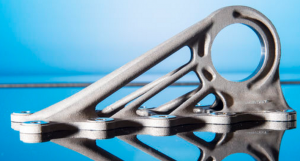
Using an example many people have seen already in the AM industry, the weight optimized airplane bracket, I decided to take a look both at the outside and in the inside of this part… since one of our associates was so kind as to print it – and yet another to CT scan it.

Some quick notes before I continue, yes you still need a machine shop to finish a part like this and no my part isn’t as pretty as the one in the image because it was extracted and cut loose from its build platform only. No polishing, de-burring, machining or inserts – just the raw data… CT scanned. At this point I must also say that this is an individual effort on my part to espouse the virtues of this type of inspection – not marketing for the company I work for or disrespect to the AM industry.
In the video below, you will see some captions; they are pretty self explanatory although a bit brief. The one section of the video that many people are probably not to up to speed on is the analyzed/visualized porosity (voids) left by the AM process. Those little colored splatters are actually inside the part and the part itself has some transparency applied so you can see these colorized defects inside.
As I said before, not all parts are perfect and many are produced with known defect/failure criteria that will perform just fine for their intended use.
So why did I post this article?
Simple; I like to share the world I live in, and that means sharing what is inside some of the data that comes across my desk, like AM parts. While CT is a growing industry, few are aware this technology is the only way to visualize what is happening with a part after it has been printed. Yes, there are some methods of in situ imaging at the present time, but they only capture the current layer and things may happen to layers below – including delamination, gas pockets and melt through.
So taking a look inside, is not only cool, it will be a requirement as this industry approaches the requirement standards that all other manufacturing processes adhere to – eventually.


